India and EU Forge Strategic Alliance to Strengthen Semiconductor Industry
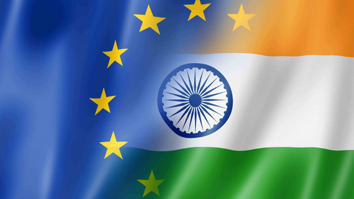


In a groundbreaking move, India and the European Union (EU) have joined forces to enhance collaboration in the semiconductor industry through a Memorandum of Understanding (MoU). The partnership aims to bolster supply chain resilience and advance research and development in semiconductors. Key areas of focus include skill development, transparency in subsidies, and the establishment of a working mechanism for efficient communication.
Resilient Supply Chains and Investments
The agreement underscores a commitment to fostering resilient supply chains by encouraging investments, joint ventures, and technology partnerships. Both parties plan to organize workshops and other initiatives to identify opportunities for collaboration in the development of semiconductor technologies, including advanced packaging, design, and raw materials. The collaboration extends to universities, research organizations, industry leaders, and other stakeholders in India and the EU.
Semiconductor Research and Development
A cornerstone of the partnership is the intention to collaborate on research, development, and innovation in semiconductor technologies. The participants aim to identify specific areas of mutual benefit, such as advanced packaging technologies and sustainable semiconductor value chains. The collaboration seeks to promote research initiatives that contribute to the long-term growth and sustainability of the semiconductor industry.
Advanced Skills Development
Recognizing the crucial role of skilled professionals in the semiconductor industry, the participants are set to establish deep cooperation in promoting advanced skills. The focus includes talent and workforce development, with an emphasis on sharing knowledge of skills programs in both India and the EU. This initiative aims to equip individuals with the expertise required to thrive in the dynamic semiconductor sector.
Transparency in Subsidies
Addressing the need for transparency, the participants commit to sharing specific information about public support in the semiconductor sector. A dedicated working group, WG1, will facilitate the exchange of information on public support granted by each party. This move aims to increase transparency and foster an environment conducive to fair and equitable collaboration.
Working Mechanism and Participation
The MoU outlines a clear working mechanism with the CEO of India Semiconductor Mission serving as the point of contact from the Indian side and the Director of Directorate A of DG CNECT representing the European Commission. Regular meetings, both virtual and in-person, are slated to occur annually to facilitate ongoing collaboration and progress updates.
Encouraging industry and stakeholder engagement, the participants express their intention to involve the private sector in both jurisdictions. Additionally, considerations for involving non-governmental stakeholders, such as businesses, trade associations, and academic and research institutions, will be explored as appropriate.
This strategic alliance marks a significant step toward fostering global cooperation in the semiconductor industry, combining the strengths of India and the EU for mutual benefit and technological advancement.


Comments